RISING BLACKS EXPLAINED
Note - following information is speculation based on patent and journal information
Brief Version
Effect - The more the panel is used the higher the black level (MLL) becomes.
Cause - The panel is programmed to increase initialization voltage as hours used increase.
Reason - As the panel is used the Magnesium Oxide (MgO) material inside each pixel is damaged by high energy ions. The MgO material is essential in determining the voltage at which the pixels can stably operate. As MgO becomes damaged more voltage is required to generate fast and stable discharge of the gas.
Why only Panasonic - Other manufacturers compensate for MgO damage by increasing address voltage or width rather than messing with initialization voltage.
- Increasing Initialization voltage compensates for MgO damage by increasing the intensity of the priming electron emission and thus lowering the discharge start voltage thus enabling stable addressing and no misfiring of pixels. Efficiency is maintained but black level suffers.
- Increasing Address voltage or width compensates for MgO damage by directly increasing the discharge probability of the address step and thus enabling stable addressing and no misfiring pixels. Black level is maintained but efficiency suffers.
Panasonic may have chosen the initialization method to save efficiency (power and brightness). Pioneer claims that the single crystal MgO they use (Crystal Emissive Layer) is not easily damaged and thus does not require voltage adjustments.
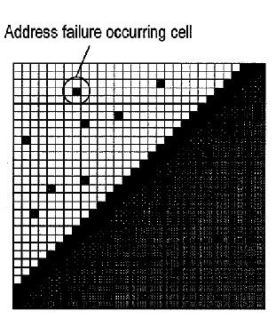
A graphic describing
misfiring pixels - what happens without RISING BLACKS (or FLOATING BLACKS)
 Detailed Version
Sorry for the lengthy post. I thought I would summarize the scientific evidence we have found into one single post as a reference. There will be a link to this post in the zero black sticky as “related material” and I also recommend a link in the first post of this thread.
While Panasonic has a few patents on the subject they do not clearly state the source of the issue. However, there is ample evidence in the literature (patents and journals) to make a good educated guess.
Panasonic Patent application #20090021452 – describing a raise in initialization voltage as power on accumulated time increases. Detailed description found
HERE
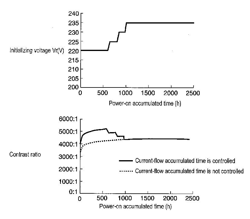 Panasonic Patent application #20090303222
 – describes that conventionally the address voltage or scan width is raised to compensate for material changes within the cell. Instead Panasonic chose to increase the initialization pulse which changes black level.
But why is it necessary?
When this issue came to light more than a year ago I proposed that the root cause was material changes (specifically MgO) within the cell over time. Several publications in IDW and SID journals either mention or go into detail on this subject and provide evidence to support this theory.
Important parameters
- Discharge Delay – time lapse from voltage application to discharge of the gas (want it minimized)
- Discharge Probability – probability the gas will discharge when voltage is applied (want it maximized)
In order to have stable operation of a modern PDP these parameters need to be stabilized or compensated for. In other words voltage changes over time are to stabilize or compensate for these parameters.
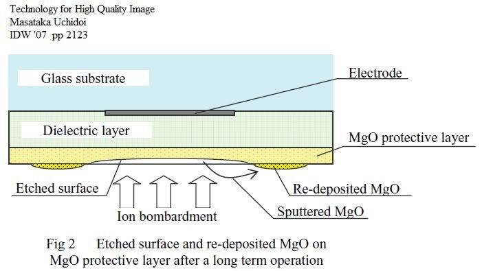
The most common reason why these parameters change is the same reason why PDP has long lasting IR problems. That reason being MgO sputtering. Even though MgO is sputter resistant it still will sputter and redeposit onto the cell walls over time and even onto the phosphor material. Below is a graphic from a Pioneer paper describing how this happens over time. Notice how the MgO has sputtered away onto the adjacent MgO on the dielectric layer.
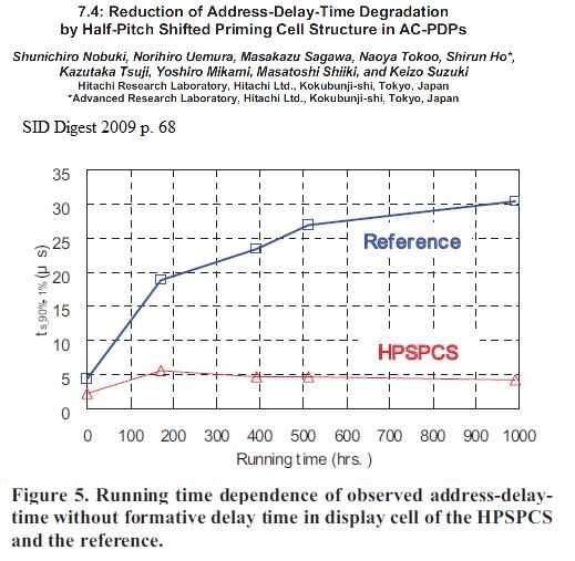
This can have a negative effect on discharge delay and probability. If the discharge delay is increased and the probability is decreased the cell may start to misfire (not discharge when voltage applied). Below is a graphic from Hitachi paper describing how the discharge delay goes up (bad news) with usage time. They also state the reason being MgO sputtering. The "Reference" sample is the one you look at. The other plot (HPSPCS) is a new cell designed to reduce this problem (more on that later).
 Why does only Panasonic have a black level rise?
The most obvious reason is that other manufacturers may have chosen to raise address voltages or widths to compensate instead of messing with initialization (see patents above).
To What benefit? Well it can be speculated that since REAL BLACK DRIVE uses initialization (selective) for every subfield (10 times a frame) that raising the address voltage or width will increase power and/or reduce the time available for light emission. In other words the display will be less efficient. If voltage changes to the all-cell initialization are used instead, then the discharge delay and discharge probability can be kept stable without long term changes to panel efficiency. This may be the “FEATURE” they speak of. Unfortunately the black level is impacted.
Aside from that see below:
Interestingly the Hitachi paper (below) describes a new cell design with a separate priming cell that prevents degradation of the MgO layer and stabilized the discharge delay over long running times (similar to the Pioneer and Panasonic designs mentioned in the zero black thread)
Also, interestingly the Pioneer paper (below) also states that the CEL – crystal emissive layer essentially blocks the degradation of the MgO layer above it and prevents any change in characteristics which may explain why the black level is stable in Pioneer models beyond 2005 (the year CEL was introduced). Also it explains the IR resistance of the Pioneer models.
References
S. Nobuki, N. Uemura, S. Ho, M. Shiiki, and K. Suzuki,"Reduction of address delay time degradation by discharge transition from priming cell to display cell in AC-PDPs," Proceedings of The 15th IDW, 785-788 (2008).
M. Uchidoi, "Technology for high quality image," in Proc. IDW Dig., 2007, pp.
2121-2124.
; pues eso es un negro flotante. Claro que de día no se ve, pero con poca luz o ninguna en la habitación es descarado.


 LinkBack URL
 About LinkBacks


 "La necedad moderna no es la ignorancia, sino el no-pensamiento de las ideas preconcebidas."
  (Kundera)
 Citar
Citar


![]:|](http://www.forodvd.com/images/smileys/cornudo.gif)


